
Table of Contents
India’s semiconductor industry has moved from policy promise to production floor in 2026. With the ₹1.64-lakh-crore ISM 2.0 now backing 12 major projects and Micron’s Sanand facility already operational, the country is on track to create close to a million semiconductor-linked jobs.
For engineering graduates and technical learners, this is no longer a future opportunity. It’s a hiring wave happening right now.
Key Takeaways
- ISM 2.0 supports 12 projects worth ₹1.64 lakh crore.
- Micron’s Sanand ATMP plant is India’s first operational one under the mission.
- Tata Electronics’ Dholera fab targets first silicon by late 2026.
- ECE, EEE, Electrical, Instrumentation, and Mechanical graduates fit core roles.
Kickstart Your Embedded Systems Career and Turn Your Tech Passion into High-Demand Skills!
What is the Semiconductor Industry & Why is it Booming in India?
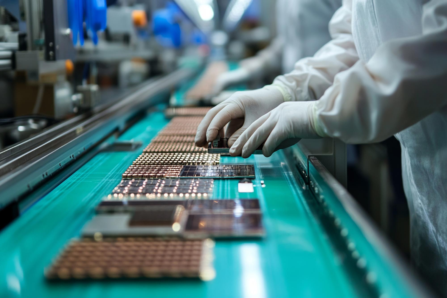
The semiconductor industry primarily covers the fabrication, design, testing, and packaging of microchips. These are basically the components that power smartphones, laptops, electric vehicles, and medical devices. India has historically consumed more chips than it manufactures.
But that balance is shifting fast, driven by
- government investment
- private capital from Tata and Micron
- global demand to diversify supply chains away from Taiwan and China
The result is a sector exclusively hiring across every skill level, from cleanroom technicians to VLSI design engineers.
Master Embedded Systems Programming!
Launch your tech career with our Embedded Systems Course, designed for hands-on learning and industry readiness.
Know MoreHow Much is India Investing through ISM 2.0?
India Semiconductor Mission 2.0 was formally launched in the Union Budget 2026-27. The first phase is built with a sharper focus on the materials, equipment used, design IP, supply chain resilience, and workforce skilling.
Under ISM (India Semiconductor Mission in full form), 12 semiconductor manufacturing projects have been approved with a combined investment pipeline of about ₹1.64 lakh crore. This includes
- 1 fabrication unit
- 2 compound semiconductor fabs
- 9 packaging (ATMP/OSAT) units
As of May 2026, the government had cleared 13 semiconductor projects across seven states under ISM and the SPECS scheme. This includes a mini/micro-LED display facility and a new packaging and testing unit.
India’s Semiconductor Mission at a Glance
| Parameter | Detail |
| Mission phase | ISM 2.0 (Union Budget 2026-27) |
| ISM 1.0 outlay | ₹76,000 crore |
| ISM 2.0 approved project pipeline | ~₹1.64 lakh crore (12 projects) |
| Projects breakdown | 1 fab, 2 compound semiconductor fabs, 9 ATMP/OSAT units |
| States with approved projects | 7 states (as of May 2026) |
| First operational facility | Micron ATMP, Sanand (Feb 2026) |
| Anchor fab project | Tata Electronics–PSMC, Dholera |
Union Electronics Minister Ashwini Vaishnaw has indicated that four plants will be operational by end-2026 and two more in 2027. On top of that, India’s first full fabrication unit at Dholera is expected by 2028.
India also unveiled Vikram, its first fully indigenous 32nm chip. This marks growing design capability alongside manufacturing.
What Semiconductor Jobs are Available in India Right Now?
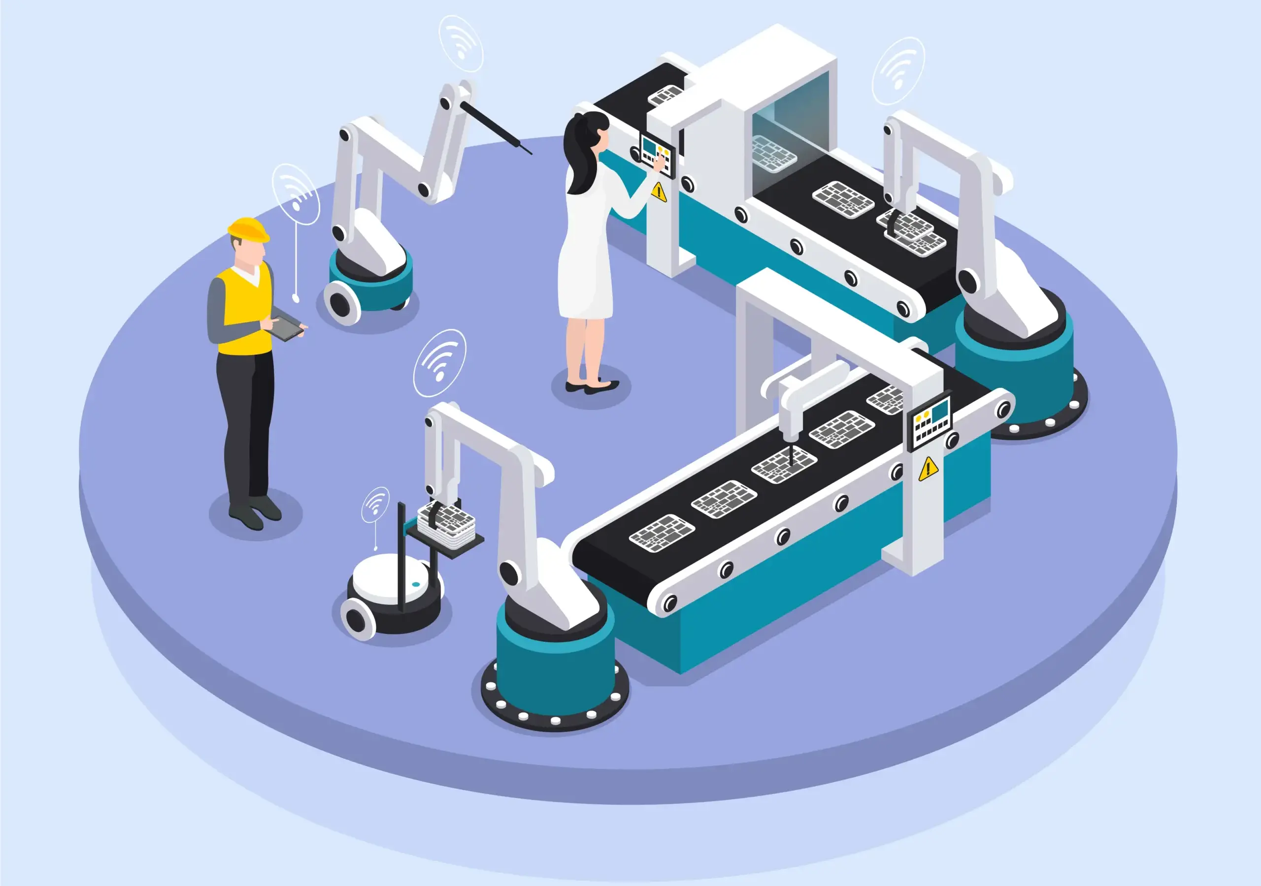
Hiring is already underway across manufacturing sites, global capability centres (GCCs), and design studios. Industry estimates suggest that the sector could generate close to 10 lakh jobs by 2026-27.
This consists of around
- 3 lakh in fabrication
- 2 lakh in ATMP
- the rest across chip design, embedded software, equipment maintenance, and supply chain management
Design hiring is a strong signal. Semiconductor design GCCs reported over 3,500 open roles by March 2026, up from ~2,400 in January.
This is pushed further by VLSI and systems/applications software roles driving most demand. Bengaluru remains the largest hub, but Hyderabad is emerging fast as GCCs expand beyond the metros.
Semiconductor Career Paths in India
| Job Area | Common Roles | Core Skills | Best Suited For |
| Chip Design | VLSI Engineer, RTL Design Engineer | Verilog/VHDL, EDA tools, digital logic | ECE, EEE, CSE graduates |
| Fabrication | Process Engineer, Equipment Engineer | Semiconductor processes, cleanroom operations | Core engineering graduates |
| Testing & Validation | Test Engineer, Validation Engineer | Debugging, test planning, quality checks | Electronics graduates |
| Packaging (ATMP) | Assembly Engineer, Packaging Technician | PCB basics, reliability testing | Diploma and degree holders |
| Support Functions | QA Specialist, Supply Chain Analyst | Quality control, logistics, procurement | Technical and management backgrounds |
What Skills do You Need for a Semiconductor Career?
Most roles combine core electronics fundamentals with industry-specific training with hands-on project experience. Recruiters consistently look for:
- Strong electronics, microprocessors, and circuit design.
- VLSI/chip tools: Verilog, RTL, EDA.
- Knowledge of semiconductor manufacturing and cleanroom protocols.
- Testing, debugging, and QA.
- Automation and equipment handling.
- Analytical, structured problem-solving.
Short-term certifications in VLSI, embedded systems, PCB design, and semiconductor process technology can help bridge the gap between an engineering degree and job readiness.
This is especially the case for candidates from ECE, EEE, Electrical, Instrumentation, and Mechanical backgrounds.
Master Embedded Systems Programming!
Launch your tech career with our Embedded Systems Course, designed for hands-on learning and industry readiness.
Know MoreWhich Companies and States are Leading India’s Semiconductor Push?

Gujarat is at the centre of India’s fab ecosystem. This is anchored by Tata Electronics’ Dholera project and Micron’s Sanand ATMP facility.
Alongside these, CG Semi, Kaynes, and Renesas are scaling packaging and testing operations. 50+ fabless design startups are supported through the Design Linked Incentive (DLI) 2.0 scheme for AI, IoT, automotive, and telecom chips.
| Facility Type | What Happens Here | Career Scope |
| Fab Units (e.g., Dholera) | Wafer production and chip fabrication | High-skill engineering and process roles |
| ATMP/OSAT (e.g., Sanand) | Assembly, testing, and packaging | Technician, engineer, and QA roles |
| Design Centres/GCCs | Chip architecture and RTL design | VLSI and software design jobs |
| Equipment & Materials | Installation, calibration, maintenance | Service and technical support roles |
| Supply Chain Hubs | Materials sourcing, logistics | Planning and coordination roles |
What are the Salary Trends in India’s Semiconductor Industry?
Compensation has scaled up fast as demand outpaces the supply. As a fresher, you can start the job typically earning between ₹4.8 LPA and ₹20 LPA. Understand that this depends on role and specialisation you choose.
Professionals with 3 to 5 years of experience, especially in design and process engineering, can often help you move into the ₹18 LPA to ₹23 LPA range.
Senior specialists in analog design, RF, or AI-chip architecture at top MNCs can earn ₹40 LPA to ₹60 LPA or even more with stock and bonuses.
What Challenges does the Industry Face?
The structural challenges include
- High capital costs
- Long fab-commissioning timelines
- Heavy dependence on imported equipment and specialty materials
Talent is a bigger constraint. India needs to upskill several lakh professionals annually to keep pace with fab and ATMP expansion.
For job seekers, this gap is an advantage – candidates who build practical, tool-specific skills early have a real edge.
Kickstart Your Embedded Systems Career and Turn Your Tech Passion into High-Demand Skills!
What does the Future Look Like Beyond 2026?
The good news is that the hiring curve is only getting steeper. This is especially true with four plants expected to be operational by end-2026, two more in 2027, and India’s first full-scale fab targeted for 2028.
India is also aiming for 70% to 75% self-sufficiency in domestic chip demand by 2029. For students and early-career professionals, semiconductor skilling is fast. It has, in fact, become one of the most future-proof bets in Indian technical education.
Conclusion
India’s semiconductor story in 2026 is no longer simply a policy headline. It is an active, fast-scaling job market.
Between ISM 2.0’s investment pipeline, operational facilities like Micron’s Sanand plant, and a design ecosystem hiring every month, the sector offers a rare mix of manufacturing-scale job volume and high-value engineering roles.
For ECE, EEE, Electrical, and Mechanical graduates and technicians willing to build hands-on skills, this is a genuinely rewarding time to enter the industry.
Master Embedded Systems Programming!
Launch your tech career with our Embedded Systems Course, designed for hands-on learning and industry readiness.
Know MoreFrequently Asked Questions
Which engineering branches suit semiconductor jobs best?
ECE, EEE, Electrical, Instrumentation, and Mechanical graduates are best positioned for core roles. Diploma holders can also enter through technician-level packaging and testing positions.
Which companies are leading semiconductor manufacturing in India?
Tata Electronics, Micron, CG Semi, Kaynes, and Renesas are among the key players building fabs, ATMP units, and packaging facilities. Tata’s Dholera fab, developed with Taiwan’s PSMC, is the mission’s anchor project.
Which Indian states have the most semiconductor investment?
Gujarat leads with the Dholera fab and Sanand ATMP facility, followed by growing activity across seven states with approved ISM projects. Karnataka and Telangana remain strong hubs for chip design GCCs.
What skills are most in demand for semiconductor jobs?
VLSI design, RTL coding, semiconductor process knowledge, and testing/validation skills are consistently in demand. Familiarity with EDA tools and cleanroom protocols is a strong added advantage.
Are freshers eligible for semiconductor industry jobs?
Yes, freshers are actively hired into design, testing, packaging, and process roles, especially through GCCs and ATMP facilities. Internships and certification courses can meaningfully improve placement chances.
When will India's first semiconductor fab be operational?
Tata Electronics’ Dholera fab is targeting first silicon by late 2026, with the plant expected to be fully operational by 2028. Micron’s ATMP facility in Sanand is already operational as of February 2026.
What are the biggest challenges facing India's semiconductor industry?
High capital costs, import dependence on specialised equipment, and a persistent talent shortage are the industry’s main hurdles. Bridging the skills gap through targeted training remains a top priority.
How can I start a career in the semiconductor industry?
Begin with a strong electronics foundation through an engineering degree or diploma, then build practical skills via VLSI, embedded systems, or process technology certifications. Hands-on internships with fabs, ATMP units, or design GCCs significantly improve entry-level job prospects.