
Table of Contents
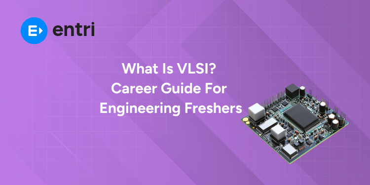
VLSI, Very Large-Scale Integration in full form, is basically a branch of electronics engineering. It is about designing integrated circuits that pack millions to billions of transistors onto a single silicon chip.
This is, in fact, now at the centre of every smartphone processor, AI accelerator, and automotive control unit that is being built.
India’s semiconductor manufacturing push has crossed billions in approved investment. In that scenario, VLSI has become one of the fastest-growing entry points for engineering graduates in ECE, EEE, and related branches.
Kickstart Your Embedded Systems Career and Turn Your Tech Passion into High-Demand Skills!
Key Takeaways
- VLSI is about chip design from idea to silicon.
- Freshers join via RTL, verification, physical, DFT, or analog/layout.
- India’s fabs (Tata-PSMC Dholera; Micron/CG Sanand; Tata Jagiroad) boost hiring. Most design work stays in MNC centres.
- Verilog, digital logic, Python/Tcl beat degrees for interview access.
- Fresher pay: ~₹4 LPA to ₹6 LPA (services) to ₹15 LPA+ (top product).
- 6 to 12 months (RTL → verification → basic physical) readies you for interviews.
- Early specialization (UVM, physical, DFT) speeds growth.
What does a VLSI Engineer Actually Do?
A VLSI engineer’s core job is about taking a chip from a mere concept to silicon through a defined pipeline. This includes:
- Specification
- RTL (register-transfer level) coding
- Synthesis
- Place-and-route
- Timing signoff
- GDSII handoff for fabrication
Engineers usually write hardware description code in Verilog or VHDL. Then it verifies through simulation and then hand it off through synthesis and physical design tools.
This is before it becomes an actual chip layout. This is not really software development. A bug caught after fabrication can cost lakhs to fix. This is exactly why verification and testing carry so much weight in the field.
Master Embedded Systems Programming!
Launch your tech career with our Embedded Systems Course, designed for hands-on learning and industry readiness.
Know MoreWhy VLSI Careers are Gaining Momentum in 2026
India’s chip ecosystem has moved from policy announcements to physical infrastructure. Micron’s assembly and test facility in Sanand, Gujarat became operational in early 2026, and the Tata-PSMC wafer fabrication plant at Dholera.
This is India’s first full-scale 300mm fab, which has crossed the halfway construction mark, with trial production targeted for late 2026. Alongside these, Tata Electronics’ packaging unit in Jagiroad, Assam, and CG Power’s OSAT facility in Sanand are already running.
More than a dozen semiconductor-related projects have been approved across seven states under the India Semiconductor Mission.
Beware of these
It’s worth being clear-eyed about what this means for freshers: these fabs mostly need manufacturing, process, and equipment engineers, not RTL or verification engineers.
The bulk of VLSI design hiring with RTL, verification, physical design, DFT still happens at global design centres of companies like
- Qualcomm
- Intel
- Texas Instruments
- Samsung
- AMD,
These have had large India teams for years.
What the mission does is build public and investor confidence in the sector, push more colleges to offer VLSI specializations, and create a genuine domestic talent pipeline that companies are now competing for.
Entry-Level VLSI Roles for Freshers
| Role | Core skills required | Typical first-year work |
| RTL / Digital Design Engineer | Verilog/VHDL, digital logic, basic Python/Tcl | RTL coding, unit-level simulation, bug fixes |
| Verification Engineer | SystemVerilog, UVM basics, simulation tools | Writing testbenches, running testcases, debugging |
| Physical Design Engineer | Place-and-route basics, timing awareness | Floorplanning, running P&R flows, DRC/LVS cleanup |
| DFT Engineer | Scan chain theory, ATPG basics | Inserting test structures, fault analysis |
| Analog/Layout Engineer | CMOS fundamentals, layout tools | Schematic-to-layout work, LVS/DRC iterations |
Career progression typically runs
Junior Engineer → Engineer → Senior Engineer → Lead/Architect
This has a branch into EDA tool development, IP leadership, or management at senior levels.
Moving between tracks like from RTL into verification is common after a year or two of focused upskilling.
Skills Freshers should Prioritize
The right sequence of skills gets you interview calls faster than grades alone:
- Digital logic and CMOS basics – gates, timing, setup/hold, metastability.
- Verilog as your primary HDL, with VHDL as a bonus.
- Simulation and verification –simulator basics, then SystemVerilog and UVM concepts.
- Synthesis and constraints – understanding SDC files and common synthesis pitfalls.
- Scripting – Python for data handling, Tcl for EDA tool automation.
- Physical design awareness – placement, routing, clock trees, static timing analysis.
- DFT fundamentals – scan chains, ATPG essentials.
- Analog basics – MOS transistor behaviour, for those eyeing analog/RF roles.
- Documentation and Git – a well-maintained GitHub of RTL projects matters more than most freshers realize.
Master Embedded Systems Programming!
Launch your tech career with our Embedded Systems Course, designed for hands-on learning and industry readiness.
Know MoreA Realistic 3–6–12 Month Roadmap
First 3 months:
Learn digital logic and Verilog. Build small RTL modules like counters, adders, FSMs. Document every project on GitHub.
Months 4 to 6:
Learn synthesis basics and run simple synthesis flows. Study SystemVerilog and write basic UVM-style testbenches. Start scripting with Python and Tcl.
Months 7 to 12:
Explore physical design fundamentals such as
- Placement
- Routing
- Timing closure
If institutional tools are not accessible, you can use open-source flows like OpenROAD. Attempt an end-to-end mini-project:
RTL → Simulation → Synthesis → Basic P&R
Apply for internships and off-campus roles while preparing for interviews.
VLSI Salary in India for Freshers (2026)
Fresher pay in VLSI varies more by company tier than almost any other engineering field. The average VLSI Design Engineer salary sits around ₹7 LPA, with a typical range between roughly ₹4.3 LPA and ₹13.5 LPA depending on company and location. Top earners even report figures above ₹22 LPA.
| Company type | Typical fresher CTC range |
| Global product companies (Intel, Qualcomm, TI, Samsung) | ₹15–24 LPA |
| EDA tool companies (Synopsys, Cadence) | ₹12–20 LPA |
| Indian design services / semiconductor services firms | ₹4–10 LPA |
Treat any single average number with caution. The spread between a services-firm offer and a top MNC design-centre offer for the same fresh graduate can be three to four times.
Specializing in verification (UVM) or advanced-node physical design tends to command a premium as experience builds. This is especially since these skills directly reduce the cost of design errors.
Where Freshers get Hired
Hiring happens through campus placements, internships, off-campus drives, and referrals through alumni networks and LinkedIn.
Employers span global product companies with India design centres, EDA vendors, semiconductor design-services firms, and increasingly, companies building out roles around India’s new fab and packaging facilities.
A well-documented GitHub portfolio consistently outperforms a plain resume in this field.
Common Challenges for Freshers & How to Handle them
Limited tool access:
Use academic licenses, cloud labs, or open-source alternatives like OpenROAD for physical design practice.
Theory-practice gap:
Short, focused courses on CMOS and transistor-level concepts can close this quickly. You don’t need a full semester to refresh fundamentals.
Long tool runtimes:
Scale down to smaller test cases while learning, and automate repetitive checks with Python or Tcl scripts.
Interview readiness:
Mock interviews focused on RTL coding, timing questions, and basic verification scenarios matter more than memorizing definitions.
Kickstart Your Embedded Systems Career and Turn Your Tech Passion into High-Demand Skills!
Conclusion
VLSI offers Indian engineering freshers a rare combination. You actually have a strong entry-level demand with a genuine specialization ladder. It holds a growing domestic ecosystem backed by real fab and packaging infrastructure coming online through 2026 and beyond.
The field does not reward degrees alone. It rewards freshers who can show a working RTL project, explain a timing bug they debugged, or walk through a basic verification testbench.
Start with Verilog and digital logic. Then work on building one small end-to-end project. You can then use the 3-6-12 month roadmap to structure your learning before you start applying.
Master Embedded Systems Programming!
Launch your tech career with our Embedded Systems Course, designed for hands-on learning and industry readiness.
Know MoreFrequently Asked Questions
Is VLSI a good career for freshers in 2026?
Yes. India’s expanding semiconductor mission and steady global design-centre hiring are creating consistent entry-level demand. Success depends more on demonstrable project skills than on the degree alone.
Which branch is best for a VLSI career?
Electronics and Communication Engineering (ECE) and Electrical Engineering (EEE) graduates have the most direct path, since VLSI builds on digital logic and circuit fundamentals from these branches. Computer Science graduates can also enter through strong RTL and scripting skills.
How is VLSI different from embedded systems?
VLSI focuses on designing the chip itself at the circuit and layout level, while embedded systems focuses on programming and integrating hardware that uses existing chips. The choice depends on whether you prefer circuit-level design or software-hardware integration.
Can a computer science graduate switch to VLSI?
Yes, though it requires deliberately learning digital logic, Verilog, and basic circuit concepts that aren’t part of a typical CS curriculum. Building hands-on RTL projects is the fastest way to bridge this gap.
Which companies hire VLSI freshers in India?
Global product companies with India design centres, EDA tool vendors, and semiconductor design-services firms are the primary hirers. Newer manufacturing and packaging facilities coming up under India’s semiconductor mission are also creating adjacent roles.
What programming languages should I learn for VLSI?
Verilog is the essential hardware description language to start with, alongside Python and Tcl for scripting and automation. SystemVerilog becomes important once you move into verification roles.
How long does it take to become job-ready in VLSI?
Most motivated freshers can become interview-ready in 6 to 12 months of focused, project-based learning. This includes building RTL modules, understanding basic verification, and getting exposure to synthesis and physical design concepts.
What is the highest-paying specialization in VLSI?
Analog and mixed-signal design, along with advanced-node physical design and specialized verification (UVM with complex IP experience), tend to command the highest long-term salaries. This is largely due to the scarcity of engineers skilled in these areas.
What is the career path after entering VLSI as a fresher?
The typical progression moves from Junior Engineer to Engineer, then Senior Engineer, before branching into Lead/Architect roles or specialized tracks like EDA tool development. Movement between RTL, verification, and physical design tracks is common within the first two years.
How is India's semiconductor mission affecting VLSI hiring?
India’s semiconductor mission is building fabrication and packaging infrastructure such as the Tata-PSMC Dholera fab and Micron’s Sanand facility. This is strengthening the broader ecosystem and investor confidence. However, most VLSI design roles for freshers still come from established global design centres rather than the fabs themselves.